
1R (1 Rank / Single Rank)
A memory module configuration where all memory chips are connected to a single 64-bit wide data block. In this setup, the system accesses all chips simultaneously as one logical unit, offering lower latency and simplified power management compared to multi-rank configurations.
2R (2 Rank / Dual Rank)
A memory module design that contains two independent 64-bit wide data blocks (ranks) on the same PCB. In a dual-rank configuration, the memory controller manages these two logical sets separately, effectively doubling the data capacity accessible through the same physical slot while optimizing memory interleaving performance.
Advanced Power Shield
Advanced Power Shield is a protection technology designed to ensure data safety during power instability. When the external voltage drops to a critical level, the SSD controller immediately triggers a protection mechanism to halt host communication and flush data from the DRAM cache and mapping tables into the NAND flash. This firmware-based design prevents firmware corruption and user data loss caused by unexpected power outages. It ensures high data integrity and device reliability in industrial environments where stable power supply is not always guaranteed.
AES (Advanced Encryption Standard)
A globally recognized symmetric-key block cipher used to secure sensitive electronic data. Established by NIST as the industry standard (FIPS 197) in 2001, AES processes data in 128-bit blocks and supports key lengths of 128, 192, and 256 bits. It is renowned for its high efficiency and robust resistance against brute-force attacks, making it the primary encryption method for government, financial, and enterprise-level data protection.
AES-128
A specific implementation of the Advanced Encryption Standard (AES) that utilizes a 128-bit key length for data encryption and decryption. AES-128 undergoes 10 rounds of mathematical transformation to secure data blocks. It is widely considered the industry benchmark for secure communications, offering a perfect balance between high-level security and computational performance (speed), making it ideal for real-time encryption in hardware and mobile devices.
AES-256
The most secure variant of the Advanced Encryption Standard, employing a 256-bit key length to provide the highest level of data protection. AES-256 utilizes 14 rounds of encryption transformations, making it virtually immune to brute-force attacks even with future advancements in computing power. It is the preferred choice for protecting highly classified information, government secrets, and critical enterprise
Anti-Sulfuration
Anti-Sulfuration is a protective technology designed to prevent electronic components from being corroded by sulfur gases in the atmosphere. In environments such as industrial plants, chemical factories, or highly polluted areas, sulfur reacts with the silver electrodes in components to form silver sulfide. This "sulfuration" process increases electrical resistance and eventually leads to open-circuit failures.
To ensure reliability beyond industry norms, SP Industrial defines its own stringent internal qualification criteria, requiring compliance with ASTM B809-95 and ISA 71.04 G2 standards.
These exclusive, high-level requirements guarantee that our products remain stable and durable even in the most demanding sulfur-rich environments.
B+M-key
M.2 Universal Keying. B+M-key is a versatile M.2 physical specification featuring two notches on the connector: one at the B-key position (left, pins 12-19) and one at the M-key position (right, pins 59-66). This design ensures maximum compatibility, allowing the module to be inserted into either a B-key or an M-key socket. However, because it supports both, the interface is typically restricted to PCIe x2 or SATA speeds, making it the standard choice for general-purpose SSDs that prioritize broad system compatibility over extreme bandwidth.
Bad Block Management
A critical NAND flash management technique used to maintain data integrity and extend storage reliability. Bad blocks—areas of flash memory that can no longer reliably store data—can be present from the factory (Early Bad Blocks) or develop over time due to wear (Later/Grown Bad Blocks). Bad Block Management automatically detects, flags, and isolates these unusable areas, redirecting data to healthy spare blocks within the over-provisioned area. By preventing data from being written to compromised sectors and proactively migrating existing data to valid blocks, BBM ensures consistent performance and protects against potential data loss.
Bank
In memory architecture, a "Bank" typically describes a logical storage unit within a DRAM chip consisting of multiple rows and columns. Modern DRAM chips are organized into multiple independent banks, allowing the memory controller to perform parallel operations (such as precharging one bank while accessing another) to minimize latency. Additionally, in hardware integration, "Bank" can refer to a group of physical memory slots on a motherboard that must be populated together to support multi-channel memory architectures and fulfill the system's data bus requirements.
BCH ECC
BCH ECC is a powerful block-based error correction algorithm used to ensure data integrity in digital communications and storage systems. It excels at identifying and correcting multiple random bit errors within a specific data block. Known for its high efficiency and low-latency hardware implementation, BCH was the industry standard for NAND Flash generations (such as SLC and MLC) before the transition to LDPC.
bit
The most fundamental unit of information in digital computing and telecommunications. A bit represents a logical state with one of two possible values: 0 or 1, which correspond to the electrical states of off or on. While a single bit is the smallest increment of data, it serves as the building block for more complex data structures; for instance, a sequence of 8 bits forms one Byte, the standard unit used to measure storage capacity and memory
Byte
A standard unit of digital information consisting of 8 bits. In computing architecture, the Byte is the primary measurement used to quantify data storage capacity and memory size. A single Byte can represent a variety of data types, such as a single character, a number, or a symbol. As the fundamental building block of data processing, multiple Bytes are organized into larger scales—such as Kilobytes (KB), Megabytes (MB), and Gigabytes (GB)—to define the scale of modern electronic files and hardware specifications.
CAMM
Compression-Attached Memory Module. An innovative memory form factor originally developed to provide a thinner and more scalable alternative to traditional SO-DIMM slots in high-performance laptops. The term "Compression-Attached" refers to its unique mounting mechanism, which uses a compression connector to interface directly with the motherboard. This design eliminates the need for bulky horizontal sockets, allowing for higher memory density and improved signal integrity within slim device profiles.
CAMM2
In memory and storage architecture, a "Channel" refers to the dedicated data path between the controller and the storage components.
- In DRAM Systems: A channel represents the independent data bus (e.g., 64-bit for DDR4/DDR5) connecting the CPU to the memory modules. Multi-channel configurations (Dual, Quad, or Octa-channel) significantly increase total bandwidth by allowing simultaneous data access across multiple modules.
- In SSDs: A channel refers to the number of Flash memory chips the controller can communicate with concurrently. While entry-level SSDs typically utilize 2 or 4 channels, high-performance enterprise and datacenter SSDs leverage 8 to 16 channels to maximize I/O throughput and reduce latency.
Channel
In memory and storage architecture, a "Channel" refers to the dedicated data path between the controller and the storage components.
- In DRAM Systems: A channel represents the independent data bus (e.g., 64-bit for DDR4/DDR5) connecting the CPU to the memory modules. Multi-channel configurations (Dual, Quad, or Octa-channel) significantly increase total bandwidth by allowing simultaneous data access across multiple modules.
- In SSDs: A channel refers to the number of Flash memory chips the controller can communicate with concurrently. While entry-level SSDs typically utilize 2 or 4 channels, high-performance enterprise and datacenter SSDs leverage 8 to 16 channels to maximize I/O throughput and reduce latency.
Chip Organization / DRAM Width
Chip Organization, often referred to as DRAM Width, describes the internal data bus configuration of a memory component. It defines the number of data bits (e.g., 4, 8, or 16) that a single DRAM chip can process per clock cycle. This architecture is fundamental to determining a memory module's total rank density and its compatibility with specific processor architectures. Choosing the correct organization is critical for optimizing system stability, performance, and supporting advanced error-correction features in enterprise environments.
CL / CAS Latency
CAS (Column Address Strobe) Latency, commonly abbreviated as CL, represents the specific number of clock cycles that elapse between a memory controller issuing a read command and the moment the first bit of data becomes available. In simpler terms, it measures the "reaction time" of the memory module. For example, a module with CL32 requires 32 clock cycles to complete this process. While higher frequencies increase raw bandwidth, a lower CL value at the same frequency indicates faster data access and improved system responsiveness.
Conformal Coating
Conformal Coating is a thin, protective film applied to the surface of a PCB. It acts as a barrier to shield electronic components from moisture, dust, chemical contaminants, and extreme temperatures. By preventing corrosion and electrical shorts, this technology is essential for ensuring the long-term reliability of devices operating in harsh or outdoor environments.
Cryptochip
A specialized hardware security microcontroller designed to protect sensitive data on storage devices, such as encrypted USB drives and SSDs. The cryptochip serves as a dedicated environment for encryption key management, ensuring that cryptographic keys are generated, stored, and processed internally rather than in the system's host memory. This hardware-based isolation protects the device against sophisticated attacks, including brute-force attempts and cold-boot exploits. By maintaining a distinct boundary between the encrypted data and the security credentials, cryptochips provide a higher level of assurance for government, military, and enterprise-grade security applications.
CSODIMM
CSODIMM is a specialized memory form factor introduced to support the high-speed requirements of DDR5 technology starting at 6400MT/s. According to JEDEC standards, these modules incorporate a dedicated Client Clock Driver (CKD). The CKD acts as a buffer that regenerates and stabilizes the clock signal sent from the CPU's memory controller before distributing it to the DRAM chips. By minimizing signal degradation and timing jitter, CSODIMM ensures system stability and enables the memory to reach higher frequencies that were previously unattainable with traditional unbuffered SODIMM designs.
CUDIMM
CUDIMM is a next-generation desktop memory standard designed to push DDR5 performance boundaries beyond 6400MT/s. In compliance with JEDEC specifications, CUDIMMs integrate a Client Clock Driver (CKD) directly onto the module. This component functions by buffering and resynchronizing the clock signal from the CPU before it reaches the DRAM chips, effectively shielding the signal from interference and degradation at extreme speeds. This architectural shift ensures superior system stability and unlocks the potential for higher overclocking frequencies in enthusiast-grade and professional desktop systems.
Data Rate
In modern memory architecture, Data Rate identifies the operational throughput of a module, measured in MT/s (Megatransfers per second). This metric has superseded "frequency" as the standard for defining DDR performance. For example, a DDR5-6400 module signifies the capability to execute 6,400 million data transfers per second across each data line. By leveraging Double Data Rate (DDR) technology—which transmits data on both the rising and falling edges of the system clock—the effective data rate reaches twice the physical clock frequency, enabling the massive bandwidth required for next-generation computing and AI workloads.
DataGuard
DataGuard is an SP proprietary, hardware-based security feature that provides immediate control over data protection and erasure. It utilizes a specific physical connector or jumper on the device's pin header to trigger functions such as Write Protect and Quick Erase. This hardware-level implementation ensures that data security can be managed independently of the host operating system, offering a reliable and flexible solution for safeguarding sensitive information in industrial and embedded environments.
DDR / Double Data Rate / DDR SDRAM
DDR stands for Double Data Rate Synchronous Dynamic Random Access Memory. The defining characteristic of DDR technology is its ability to transfer data on both the rising and falling edges of the system clock signal. Compared to legacy SDRAM, which only transmits data once per clock cycle, DDR effectively doubles the bandwidth without increasing the clock frequency. Since its inception, the DDR standard has undergone multiple generational evolutions (DDR2 through DDR5), with each iteration significantly reducing power consumption (operating voltage) while drastically increasing data transfer rates and density to meet the escalating demands of modern computing environments.
DDR3
DDR3 represents the third generation of DDR SDRAM technology, introducing significant improvements in power efficiency and bandwidth over its predecessor, DDR2. Operating at a reduced standard voltage of 1.5V, DDR3 provided a more sustainable solution for mobile and enterprise environments at its launch. The architecture enabled data transfer rates ranging from 800MT/s to 2133MT/s. While succeeded by newer generations, DDR3 remains a critical standard in legacy industrial systems and embedded applications due to its proven reliability and lower thermal profile compared to earlier memory types.
DDR3L
DDR3L is a low-voltage sub-specification of the DDR3 JEDEC standard, specifically engineered to optimize energy efficiency. While maintaining the same speed and timing performance as standard DDR3, DDR3L operates at a reduced voltage of 1.35V, significantly extending battery life in mobile devices and minimizing thermal output in high-density server environments. A key feature of DDR3L is its dual-voltage capability, which ensures full backward compatibility with legacy systems. When installed in a standard DDR3 environment or mixed with 1.5V modules, the DDR3L module automatically toggles its operating voltage to 1.5V to ensure system stability.
DDR4
DDR4 is the fourth generation of DDR SDRAM, establishing a long-standing balance between high bandwidth and robust power efficiency. Operating at a baseline of 1.2V, it covers a comprehensive speed range from 2133MT/s up to 3200MT/s. While mainstream PCs favor 3200MT/s, frequencies like 2133, 2400, and 2666MT/s remain essential standards in industrial and embedded systems for their proven stability and compatibility with long-lifecycle processors. Physically, DDR4 features a curved bottom edge on the DIMM to reduce insertion force and protect the circuit board from mechanical stress during installation.
DDR5
DDR5 is the fifth generation of DDR SDRAM, engineered to meet the extreme bandwidth demands of modern AI, high-performance computing, and enterprise data centers. Launched with a baseline of 4800MT/s, the standard now scales beyond 8000MT/s. DDR5 introduces three fundamental architectural shifts:
- Power Management: Operating at a lower 1.1V, DDR5 moves power regulation from the motherboard to the module via an onboard Power Management IC (PMIC), ensuring more granular and efficient power distribution.
- Channel Efficiency: Each module is divided into two independent 32-bit sub-channels, which, combined with doubled bank groups and burst length (BL16), significantly optimizes data access efficiency.
- Enhanced Reliability: For the first time, On-die ECC (Error Correction Code) is integrated directly into the DRAM silicon, correcting bit errors within the chip to maintain high data integrity at extreme speeds.
Debug Access Port (DAP)
Debug Access Port (DAP) is a hardware-level interface that serves as a bridge between external debugging tools and the controller's internal core. During the development phase, it allows engineers to monitor register status and firmware execution in real-time without interrupting system operations, significantly enhancing troubleshooting efficiency.
To balance development flexibility with data security, SP Industrial implements strict control requirements for this interface. Once a product enters the mass production stage, DAP access is disabled via hardware locking mechanisms to prevent unauthorized external commands from accessing sensitive data. This design ensures that the product provides industrial-grade security while maintaining advanced diagnostic capabilities during its development lifecycle.
DIMM / Dual In-line Memory Module
DIMM stands for Dual In-Line Memory Module. Unlike older SIMM (Single In-line Memory Module) technology, a DIMM features independent electrical contacts on both sides of the module, allowing for a wider and more efficient data path. Modern DIMMs typically provide a 64-bit data bus (or two 32-bit sub-channels in DDR5) to the CPU. As the standard form factor for desktop computers, workstations, and servers, DIMMs are designed to fit into motherboards with full-sized memory slots, offering higher capacities and better thermal dissipation compared to smaller form factors.
DRAM / Dynamic Random Access Memory
DRAM is the most prevalent type of volatile semiconductor memory used for active data processing in modern computing. The term "Dynamic" refers to the technology's reliance on capacitors to store data as electrical charges. Because these charges naturally leak over time, the memory must be refreshed millions of times per second to retain its stored information. Architecturally, DRAM is structured in a high-density grid of transistors and capacitors, where each cell represents a binary "1" or "0." This design balances high storage density with cost-effectiveness, making it the primary technology for system memory (RAM) in everything from smartphones to enterprise servers.
Dual Channel
Dual Channel is a system-level memory architecture that utilizes two independent data paths to aggregate bandwidth, significantly enhancing system performance. By installing a pair of identical memory modules into specific motherboard slots, the memory controller can access a 128-bit data bus (combining two 64-bit paths) instead of the standard 64-bit bus.
- In DDR4 and earlier: Performance is optimized when modules are installed in matched pairs, doubling the peak theoretical bandwidth.
- In DDR5: While a single module already features two internal 32-bit sub-channels, a dual-channel configuration further expands this to four sub-channels, providing the massive data throughput required for modern multi-core processors and data-intensive tasks.
Dual-port
In a Dual-port configuration, the interface is split into two independent paths, each using two PCIe lanes (e.g., Dual Gen4 x2). This enables "Active-Active" or "Active-Passive" high-availability, allowing two separate host controllers to access the drive simultaneously for redundancy and failover.
Dynamic Data Refresh
Dynamic Data Refresh is a proactive NAND management feature designed to maintain data integrity in SSDs, particularly against Read Disturb and Data Retention challenges. During read operations, the controller monitors the health of data blocks through a multi-stage evaluation:
- Monitoring: Each read command triggers a check for "need to refresh" flags or elevated error bit rates.
- Assessment: The controller analyzes the current Raw Bit Error Rate (RBER) and the number of Read Retries required to access the data.
- Action: If a block exceeds predefined safety thresholds, the controller automatically relocates the data to a fresh block and marks the old one for erasure. This background process ensures that data remains accessible and error-free, even in read-intensive environments, without requiring user intervention.
ECC / Error Correction Code
Error Correction Code. ECC is a sophisticated mathematical algorithm used to detect and correct data corruption within a system. In memory environments, it ensures high reliability by identifying and fixing single-bit errors (and detecting multi-bit errors) that can be caused by electrical interference or cosmic rays.
- System-Level ECC: Featured in server and workstation platforms, this requires a memory controller that supports ECC and specialized modules with additional data width (typically 72-bit for DDR3/DDR4, and 72-bit or 80-bit for DDR5) to store parity bits. This ensures data integrity between the CPU and the memory.
- DDR5 Innovation: Unlike previous generations, all DDR5 DRAM chips feature On-die ECC, which corrects errors within the chip itself. However, for true enterprise-grade protection, "ECC modules" (such as ECC UDIMM or RDIMM) are still required to provide system-level protection across the entire data bus.
ECC Engine
Error Correction Code Engine.An ECC Engine is a dedicated hardware component integrated within a Flash memory controller or a memory management unit. Its primary function is to automatically detect and correct data corruption that may occur during the reading, writing, or transmission process. By utilizing mathematical algorithms (such as BCH or LDPC), the ECC Engine ensures that the data retrieved from the storage medium matches the original data bit-for-bit. This hardware-based processing is essential for maintaining system stability and preventing data loss in high-density storage environments.
ECC UDIMM/ECC CUDIMM/ECC SODIMM/ECC CSODIMM
ECC Unbuffered modules are high-reliability memory solutions that incorporate additional DRAM components (widening the data bus to 72 or 80 bits) to support Error Correction Code algorithms. They provide server-grade data integrity while maintaining the low latency of unbuffered architecture.
- ECC UDIMM: The standard full-sized module for workstations and entry-level servers.
- ECC CUDIMM (Clocked UDIMM): A new DDR5 standard that integrates a Clock Driver (CD) directly on the UDIMM. By regenerating the clock signal on the module, it overcomes signal integrity bottlenecks, allowing for much higher stable frequencies (e.g., 6400MT/s and beyond).
- ECC SODIMM: The small form-factor version designed for high-end laptops, micro-servers, and industrial PCs (IPC) that require ECC protection.
- ECC CSODIMM (Clocked SODIMM): The compact equivalent of CUDIMM, utilizing a Clock Driver to ensure timing precision and stability at the extreme speeds of next-generation small-form-factor computing.
EEPROM
Electrically Erasable Programmable Read-only Memory. EEPROM is a type of non-volatile storage component integrated onto memory modules. Unlike DRAM, it retains its data even when power is removed. Its primary function in memory technology is to host the SPD (Serial Presence Detect), which contains critical parameters such as timing, voltage, and frequency specific to that module. During the system's power-on self-test (POST), the BIOS reads the EEPROM to automatically configure the memory controller, ensuring seamless compatibility and optimal performance between the module and the motherboard. In DDR5, the EEPROM functionality is often integrated into the SPD Hub for enhanced management.
E-key
M.2 Socket 1. E-key is a physical interface specification for M.2 modules, featuring a notch located on the left-center of the connector (pins 24-31). It is primarily designed for wireless connectivity cards, supporting PCIe x2, USB 2.0, I2C, and UART interfaces. This keying is commonly used for Wi-Fi, Bluetooth, and NFC modules in laptops and motherboards, preventing the accidental insertion of SSDs or other incompatible expansion cards into communication-specific slots.
End-to-End Data Protection
End-to-End Data Protection is a technology that ensures data integrity throughout the entire transfer process. From the moment data is sent by the host, through the controller buffer, until it is written into the NAND Flash, the system applies error-checking codes (ECC) at every stage. This mechanism detects and corrects errors occurring at any point in the internal data path, preventing corruption during transit and guaranteeing that every bit of data remains consistent and accurate from entry to storage.
FAT
FAT is a classic file system architecture originally developed to manage data organization on storage media. It utilizes a central table to track the cluster locations of files. Due to its lightweight structure and universal compatibility, FAT (including FAT32 and exFAT) remains the industry standard for cross-platform data exchange. It is the primary file system for flash memory products, such as SD cards and USB drives, ensuring seamless operation across different operating systems (Windows, macOS, Linux) and embedded devices like digital cameras and industrial controllers. While it does not directly manage NAND endurance, its simplicity makes it ideal for portable and legacy storage applications.
FIPS (Federal Information Processing Standards)
FIPS defines a series of mandatory security standards and technical guidelines established by the National Institute of Standards and Technology (NIST). While originally developed for U.S. federal computer systems, FIPS has become a global gold standard for cybersecurity in the commercial sector. In the context of data storage, these standards (most notably the FIPS 140 series) specify the requirements for cryptographic modules, covering both hardware and software implementation. Adherence to FIPS ensures that a product has undergone rigorous independent testing to verify its ability to protect sensitive data against sophisticated threats.
FIPS 140-2 Level 2
FIPS 140-2 Level 2 is an advanced security tier for cryptographic modules, building upon Level 1 requirements by adding a critical layer of Physical Security. The primary differentiator of Level 2 is the requirement for tamper-evident features, such as specialized coatings or seals that must be broken to gain physical access to the module's internal cryptographic keys. This ensures that any unauthorized attempt to physically compromise the device—such as an SSD or a secure memory module—will leave highly visible evidence of the intrusion. For enterprise and government sectors, Level 2 provides a cost-effective balance of robust software encryption and verified physical hardware protection.
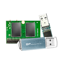
Flash Memory
Flash memory is a high-density, non-volatile electronic storage medium that can be electrically erased and reprogrammed. As a derivative of EEPROM technology, its primary advantage is the ability to retain data indefinitely without a power supply. Modern flash memory is predominantly categorized into NAND flash, which offers high capacities and fast write/erase speeds for SSDs, USB drives, and enterprise storage arrays, and NOR flash, used typically for code execution in embedded systems. Due to its lack of moving parts, flash memory provides superior durability, lower power consumption, and significantly faster access times compared to traditional mechanical hard drives (HDDs).
FrameSolid
FrameSolid is an SP proprietary firmware-based technology developed by SP Industrial to ensure long-term, stable write performance in SSDs. Unlike traditional SSDs that heavily rely on SLC cache and may experience significant speed degradation once the cache is full, FrameSolid utilizes a Direct Write mechanism combined with a specially adjusted Garbage Collection (GC) process. This ensures consistent and durable performance, preventing fluctuations that could impact system stability, making it ideal for continuous recording in surveillance systems and long-running industrial equipment.
FWxpress
FWxpress is an SP proprietary remote service solution developed by SP Industrial to simplify SSD firmware updates and optimize the technical support process. Traditionally, firmware issues required the physical return of devices (RMA), leading to significant downtime. FWxpress allows for remote, seamless firmware updates and bug fixes, significantly reducing system downtime and eliminating the need to ship hardware back. It empowers even non-technical users to perform critical updates, ensuring system stability and data security through a streamlined, efficient workflow.
Garbage Collection
Garbage Collection is a critical background management process that maintains the endurance and sustained performance of NAND flash-based storage. Because NAND cells cannot be directly overwritten, the controller must perform a Program/Erase (P/E) cycle. During GC, the controller identifies blocks containing "stale" or invalid data, relocates the remaining valid data to fresh, empty pages, and then erases the entire original block. This creates free space for subsequent writes. Efficient Garbage Collection minimizes Write Amplification (WA) and prevents performance degradation, ensuring the SSD operates at peak speeds even as it nears full capacity.
Heat Spreader / Heat Sink
A heat spreader is a specialized thermal solution, typically constructed from high-conductivity aluminum or copper, attached to memory modules or SSDs. Its primary function is to draw heat away from critical components—such as DRAM chips, NAND flash, and controllers—and dissipate it into the surrounding airflow by increasing the surface area for heat exchange. Beyond cooling, heat spreaders provide structural rigidity and protect delicate microcircuits from physical handling. In high-performance or overclocked systems, effective heat spreading is essential to prevent thermal throttling, ensuring the device maintains peak operational stability under heavy workloads.
High Bandwidth Memory (HBM)
HBM is a premium, high-performance memory architecture that utilizes 3D stacking of DRAM chips to achieve extreme bandwidth and energy efficiency. Developed to overcome the physical limitations of traditional GDDR and DDR memory, HBM connects directly to GPUs or AI accelerators via an interposer, enabling a significantly wider data bus (e.g., 1024-bit per stack). Its evolution through HBM2, HBM3, and HBM3E has seen a dramatic increase in layers and throughput. Today, HBM is the indispensable backbone of Generative AI and High-Performance Computing (HPC), providing the massive data speeds required for training Large Language Models (LLMs).
HMB Function
An NVMe feature that allows a DRAM-less SSD to utilize a portion of the system’s host memory (RAM) as its own data lookup table (Mapping Table). By leveraging the high-speed system memory to store metadata, the SSD can significantly improve read/write performance and IOPS compared to traditional DRAM-less designs that rely solely on slower NAND flash for indexing. This technology provides a cost-effective solution that brings the performance of entry-level SSDs closer to that of high-end drives with dedicated DRAM.
Industrial SSD
An industrial SSD is a high-reliability solid-state drive engineered for harsh and mission-critical industrial environments. Designed to deliver predictable and stable performance under continuous 24/7 operation, industrial SSDs are optimized for system stability and operational reliability.
Key features include wide operating temperature support, fixed BOM control, product longevity, and consistent performance stability. With strict component validation and controlled production processes, industrial SSDs are built to withstand shock, vibration, and extreme environmental conditions that standard commercial SSDs cannot tolerate.
Advanced technologies such as PFP, FrameSolid, and DataGuard further enhance data integrity, power-loss protection, and overall system reliability. Industrial SSDs are widely deployed in industrial automation, smart manufacturing, industrial control systems, and edge computing applications where longevity and dependable performance are critical.
Industrial DRAM Module
An industrial DRAM module is a memory solution specifically designed for industrial applications requiring high reliability and product longevity. Industrial DRAM modules support extended temperature ranges, including normal temperature operation from –20°C to 95°C, and wide temperature operation from –40°C to 105°C, ensuring stable performance in demanding environments. Built with validated components and designed for lifecycle stability, industrial DRAM modules are commonly integrated into industrial computers, embedded systems, and servers to maintain consistent system performance and reliable data processing under extreme thermal conditions.
LDPC ECC
Low-Density Parity-Check Error Correction Code. LDPC ECC is a sophisticated error correction algorithm used in modern Flash controllers to identify and fix data errors at the hardware level. As NAND Flash cells shrink and transition to multi-layer technologies (like TLC and QLC), they become more prone to noise and signal degradation. LDPC provides a powerful, high-performance solution that significantly increases the endurance of Flash storage by extending its Program/Erase (P/E) cycles. Its ability to perform both "Hard" and "Soft" decoding makes it the industry standard for ensuring data integrity in high-speed NVMe SSDs and advanced memory cards.
LRDIMM / Load Reduced DIMM
Load Reduced DIMM. LRDIMM is an enterprise-class memory module designed for maximum memory density in high-end servers. While RDIMMs only buffer command and address signals, LRDIMMs utilize a Memory Buffer (MB) to also buffer data signals, effectively reducing the electrical load on the memory controller. This allows systems to be populated with a higher number of high-capacity modules without forcing the controller to downclock. LRDIMM is the premier choice for memory-intensive applications like virtualization and in-memory databases, where both massive capacity and high operational frequency are required.
M.2
M.2 is a versatile small-form-factor (SFF) specification designed to replace the legacy mSATA standard. Its compact, slim profile makes it the ideal interface for ultra-thin laptops and high-performance desktops. M.2 is uniquely flexible, supporting both SATA and PCIe (NVMe) protocols, as well as non-storage expansions like Wi-Fi and Bluetooth. Modules are identified by their dimensions; for example, "2280" signifies 22mm wide and 80mm long. In the storage market, M.2 NVMe SSDs are the gold standard for high-speed data transfer, utilizing the PCIe bus to bypass the bottlenecks of traditional storage interfaces.
Mbps
Mbps is a standard unit of measurement for data transfer rates, representing one million bits transmitted per second. It is commonly used to quantify internet bandwidth and serial interface speeds. In a technical context, it is crucial to distinguish Mbps (bits) from MB/s (Bytes); since 8 bits equal 1 Byte, a transfer rate of 800 Mbps is equivalent to 100 MB/s. High Mbps ratings indicate greater throughput capacity for streaming, cloud computing, and real-time data synchronization.
MCRDIMM
Multiplexer Combined Ranks Dual Inline Memory Module. MCRDIMM is a cutting-edge DDR5 server memory architecture, backed by Intel, designed to shatter the bandwidth bottlenecks of traditional RDIMMs. The "Multiplexer" technology allows the module to access two physical ranks simultaneously, effectively doubling the data output to 128 Bytes per clock cycle. By integrating a specialized multiplexed data buffer and a Multiplexing Registered Clock Driver (MCRD), it can achieve exceptional speeds exceeding 8000MT/s. This makes MCRDIMM the ideal solution for next-generation Intel Xeon platforms handling AI training, large-scale simulations, and data-intensive enterprise workloads.
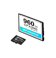
microSD Card
A microSD card is an ultra-compact, removable Flash memory form factor designed for high-density storage in space-constrained devices. While ubiquitous in consumer electronics, modern microSD cards have evolved into high-performance storage solutions capable of handling professional video workflows and industrial data logging. By leveraging advanced bus interfaces and standardized speed classes, these cards ensure the reliability and sustained throughput required for everything from mobile applications to 8K Ultra HD recording. Their robust, solid-state design makes them the preferred choice for reliable storage in mobile phones, action cameras, and IoT edge devices.
M-key
M.2 Socket 3. M-key is a physical interface specification for M.2 SSDs, characterized by a notch located on the right side of the connector (pins 59–66). It is designed to support PCIe x4 lane configurations, providing the maximum possible bandwidth for high-performance NVMe storage. M-key sockets are typically found in modern desktops and laptops to accommodate high-speed Gen 3, Gen 4, or Gen 5 NVMe SSDs, ensuring that incompatible cards (such as those requiring different voltages or bus types) cannot be inserted.
MRDIMM
Multiplexed Rank Dual Inline Memory Module. MRDIMM is a JEDEC-standard DDR5 memory architecture engineered for next-generation server environments. It achieves unparalleled data rates and bandwidth by utilizing a Multiplexed Registered Clock Driver (MRCD) and Multiplexed Data Buffers (MDB). These components allow the module to operate at twice the host interface speed, effectively doubling the transfer rate compared to conventional RDIMMs. MRDIMMs are available in two form factors: the Standard Height and the Tall Form Factor (TFF) at 56.9mm, with the latter designed for optimized cooling and capacity. First-generation modules start at 8800MT/s, with the second generation projected to reach 12,800MT/s, making them essential for AI-driven data centers and HPC workloads.
Multi-Name Space
A feature within the NVMe specification that allows a single physical SSD to be partitioned into multiple independent logical blocks, known as namespaces. Each namespace behaves as a distinct logical device with its own capacity, performance characteristics, and security attributes. This technology enables efficient resource isolation and multi-tenancy management, allowing a single drive to support different operating systems or application workloads simultaneously while minimizing resource contention.
NAND
NAND flash is a high-density, non-volatile storage technology that forms the core of modern SSDs and memory cards. Named after the “NOT-AND” logic gate, it excels in providing massive storage capacities and high-speed data access by organizing memory cells into strings and blocks. Unlike traditional DRAM, NAND retains data without power, and unlike mechanical HDDs, it has no moving parts, offering superior shock resistance. Modern NAND has evolved from 2D (Planar) to 3D NAND structures, stacking cells vertically to achieve higher bit density, improved reliability, and lower power consumption across various grades such as TLC and QLC.
Non-Volatile Memory
Non-volatile memory is a fundamental category of computer storage that retains saved data without a continuous power supply. Unlike volatile memory (such as DRAM), which clears upon system reboot or power loss, NVM provides a persistent storage environment essential for long-term data integrity. This category encompasses a wide range of technologies, from traditional NAND Flash used in SSDs to emerging Next-Generation NVM solutions. Its ability to bridge the gap between high-speed memory and permanent storage makes it the backbone of modern boot drives, firmware storage, and mission-critical enterprise data arrays.
NVM Express™ (NVMe™)
NVMe™ is a modern interface protocol designed specifically for high-speed Flash storage, such as SSDs. It connects directly to the system via the PCIe bus, allowing for much faster data transfer speeds compared to older protocols used for mechanical hard drives. By drastically reducing latency and supporting multiple data paths, NVMe™ enables your computer to boot faster, load large files almost instantly, and handle demanding tasks like video editing or gaming with ease.
On-Die ECC / ODECC
On-Die ECC (ODECC) is a built-in error-correction technology integrated directly within individual DRAM chips. Introduced with the DDR5 standard, ODECC identifies and corrects bit errors inside the chip before the data is transmitted to the rest of the system. As memory cell density increases with newer technologies, ODECC plays a vital role in maintaining data integrity and system reliability, ensuring stable performance even at the higher speeds typical of DDR5 modules.
PCI Express® (PCIe®)
PCIe® is a high-speed interface standard used to connect critical components, such as SSDs and graphics cards, to a computer's motherboard. It acts like a multi-lane highway, where more “lanes” (such as x4 or x16) allow for more data to travel at once. PCIe® performance is categorized by Generations (e.g., Gen4, Gen5), with each new version doubling the potential speed of the previous one. This makes PCIe® the essential foundation for achieving the ultra-fast transfer rates found in modern NVMe™ storage.
Power Failure Protection
Power Failure Protection is a critical safeguard designed to prevent data corruption during unexpected power loss. When a sudden drop in power is detected, the device utilizes advanced firmware—and in some cases, hardware capacitors—to immediately halt ongoing operations and ensure that data currently being written is safely committed to the NAND flash. This technology is essential for maintaining data integrity in professional and industrial environments where continuous uptime and reliable storage are paramount.
PSID
Physical Storage ID. A unique 32-character alphanumeric identifier printed on the physical label of a Self-Encrypting Drive (SED). The PSID serves as a dedicated security key designed to prove physical ownership of the device. Its primary function is to enable a “Revert” or “Sanitary Erase” command, allowing users to reset the drive and regain access in the event of a lost password or authentication failure. Note that using the PSID to reset a drive will permanently erase all stored data to ensure security.
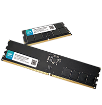
RAM / Random Access Memory
RAM, or Random Access Memory, serves as a computer's high-speed “short-term memory.” It acts as a crucial bridge between long-term storage (like SSDs or HDDs) and the processor, allowing for nearly instantaneous data access. Most modern RAM is volatile, meaning it requires constant power to retain information and clears its data once the system is turned off. Increasing the amount of RAM in a system enables smoother multitasking and faster performance for memory-intensive applications.
Rank
A Rank is a standardized data block that is 64-bits wide, forming a fundamental unit of memory that the processor can access in a single operation. It is created by combining the data widths of individual DRAM chips on a module (for example, eight x8 chips together form a 64-bit Rank). A memory module can be designed with multiple Ranks (such as Single, Dual, or Quad Rank), though the system accesses only one Rank at a time. Higher rank counts often allow for greater overall module capacity within a single slot.
RDIMM / Registered DIMM
RDIMM is a server-grade memory module that integrates a Registering Clock Driver (RCD) to enhance signal stability and system scalability. The RCD acts as a high-performance buffer between the memory controller and the DRAM components, effectively reducing the electrical load on the CPU's memory bus. This allows server platforms to support a much higher number of modules and greater overall capacities per channel. While the Register introduces a single-clock cycle of latency to synchronize command and address signals, the trade-off is essential for the rock-solid reliability required in data centers and enterprise-level computing.
Sanitize
Sanitize is a device-level security command that permanently and irrecoverably removes all user data from a storage device. Unlike standard deletion or formatting, which only remove file pointers, the Sanitize process acts on the physical storage media through methods like Block Erase, Crypto Scramble, or Overwrite. Once a Sanitize operation is successfully completed, data recovery is impossible even with advanced laboratory tools, ensuring full compliance with data privacy regulations during drive decommissioning or repurposing.
SATA
Serial Advanced Technology Attachment. SATA is a widely adopted computer bus interface designed to connect host systems to mass storage devices, such as hard disk drives (HDDs) and SSDs. As a long-standing industry standard, SATA is known for its universal compatibility and cost-effectiveness. While modern NVMe™ drives offer higher peak performance, SATA remains the ideal choice for high-capacity secondary storage, legacy system upgrades, and applications where reliability and value are the primary considerations.
SD Card
An SD card is a highly reliable, removable Flash memory form factor primarily used in digital cameras, camcorders, and professional imaging equipment. Larger in physical size than microSD cards, the SD format is preferred in high-end photography for its mechanical durability and superior heat dissipation during extended use. Modern SD cards leverage advanced interfaces and speed classes to support the rigorous demands of 4K/8K video production and high-speed burst shooting. They are a staple for creators who require consistent performance and significant storage capacity in a portable format.
SD Speed Class
The SD Speed Class is a set of standardized ratings established by the SD Association to define the minimum sustained writing speed of a memory card. These standards—including the original Speed Class, UHS Speed Class, and Video Speed Class—ensure that memory cards and host devices can work together to guarantee the performance needed for uninterrupted video recording. By identifying these symbols (such as V30 or U3), users can confidently select a card that meets the specific data throughput requirements for anything from standard HD video to professional 8K cinema-grade production.
SDRAM / Synchronous DRAM
Synchronous Dynamic Random Access Memory. SDRAM is a type of memory technology that synchronizes its operations with the system clock, allowing for efficient and high-speed data transfers. Since its introduction in the late 1990s, this “synchronous” capability has enabled the memory to time its responses perfectly with the processor's requests, eliminating unnecessary wait states. SDRAM serves as the foundational architecture for all modern DDR memory generations (from DDR1 to DDR5), making it a cornerstone of contemporary computing performance.
SFF-8639
SFF-8639 is a multi-function connector specification defined by the SFF Committee, designed to support high-performance storage interfaces including SAS, SATA, and multi-lane NVMe. It is the formal mechanical and electrical standard for the U.2 interface, featuring a high-density pin layout that accommodates up to four PCIe lanes. SFF-8639 is specifically engineered for enterprise environments, providing robust features such as hot-swapping, sideband signaling, and dual-port capability, ensuring reliable high-speed data transmission in data center servers and storage arrays.
Single-port
In a Single-port configuration, all four PCIe lanes (e.g., Gen4 x4) are dedicated to a single host path. This provides the maximum possible bandwidth for a single controller to access the SSD, maximizing sequential read/write speeds.
SMART IoT
SMART IoT is an SP proprietary, cloud-based service platform for real-time remote monitoring of SSD health status. It collects and analyzes critical S.M.A.R.T. (Self-Monitoring, Analysis, and Reporting Technology) attributes, such as erase counts and remaining lifespan, across deployed devices. By providing centralized data visualization and automated alarm notifications, SMART IoT enables administrators to perform predictive maintenance, preventing unexpected system failures and minimizing downtime in large-scale IoT and edge computing deployments.
SODIMM / SO-DIMM
SODIMM is a smaller version of a standard DIMM, designed specifically for space-constrained systems. At roughly half the length of a traditional desktop memory module, SODIMMs are the industry standard for laptops, small form factor (SFF) PCs, and high-performance networking equipment. Despite their compact size, SODIMMs offer similar performance and capacities to their full-sized counterparts, making them essential for achieving powerful computing in portable and slim-profile devices.
Speed Class (Class 4, 6, 10)
Speed Class is the original standardized rating system for SD and microSD cards, identified by a number inside a circular “C” symbol. It defines the minimum sustained write speed to ensure consistent performance for basic photography and video recording. The ratings include Class 4 (4MB/s), Class 6 (6MB/s), and Class 10 (10MB/s). While newer Video Speed Classes (such as V30) have been introduced for higher-end applications, the original Speed Class remains a helpful reference for identifying compatibility with standard-definition devices and everyday data storage.
SR-IOV
Single Root I/O Virtualization. An interface specification that allows a single physical PCIe device, such as a network adapter (NIC) or storage controller, to appear as multiple separate logical devices to a virtualized system. By implementing Physical Functions (PF) and Virtual Functions (VF), SR-IOV enables virtual machines (VMs) to bypass the hypervisor and interact directly with the hardware. This significantly reduces CPU overhead, lowers latency, and maximizes I/O throughput in high-performance computing environments.
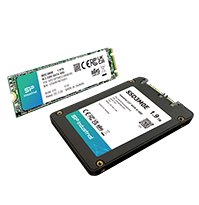
SSD
An SSD is a high-performance storage device that utilizes Flash NAND chips to store data electronically. Unlike traditional Hard Disk Drives (HDDs) that rely on spinning platters and moving mechanical parts, SSDs use an advanced controller to access data instantly. This architecture makes SSDs significantly faster, quieter, and more resistant to physical shock and vibration. With benefits like near-instant boot times and rapid file transfers, SSDs have become the standard for everything from ultra-slim laptops to massive enterprise data centers.
TCG Opal
TCG Opal is a set of specifications developed by the Trusted Computing Group for Self-Encrypting Drives (SED). It provides a hardware-based encryption standard that ensures data at rest is automatically encrypted without impacting system performance. By managing security features within the drive controller, TCG Opal offers robust protection against unauthorized access and data theft, making it a critical security requirement for corporate and government IT environments.
Thermal Throttling
Thermal Throttling is a self-protection mechanism that automatically adjusts performance when a device (e.g., SSD or DRAM) detects temperatures exceeding safe limits. By reducing the operating frequency to lower heat generation, this technology prevents hardware damage and data corruption, ensuring system stability and continuous operation even in extreme thermal environments.
U.2
U.2 is a high-performance interface standard designed primarily for enterprise and data center storage. While it shares the same 2.5-inch form factor as traditional SATA SSDs, U.2 utilizes the PCIe® NVMe™ interface to deliver significantly higher speeds and lower latency. Its larger physical size compared to M.2 allows for greater storage capacities and superior heat dissipation, making it ideal for 24/7 heavy workloads and high-density server environments that require both extreme performance and long-term reliability.
U.3
U.3 is an evolutionary interface standard based on the SFF-TA-1001 specification. It features Tri-mode functionality, allowing a single backplane slot to support NVMe, SAS, and SATA drives interchangeably through a unified wiring scheme. By consolidating different protocols onto a single set of pins, U.3 simplifies server internal cabling and provides greater flexibility for data center storage scaling without requiring separate backplanes for different drive types.
UDIMM / Unbuffered DIMM
Unbuffered Dual In-line Memory Module. UDIMM is the most common type of memory module used in desktop PCs, workstations, and gaming systems. As an “unbuffered” module, it transmits signals directly from the memory controller to the DRAM chips without an intermediate register. This direct architecture provides high speed and low latency at a cost-effective price point, making it the ideal standard for everyday computing and high-performance gaming where massive server-scale capacities are not required.
UHS Speed Class (U1, U3)
UHS Speed Class is a performance standard that defines the minimum sustained write speed specifically for video recording on UHS-compatible devices. There are two primary ratings: UHS Speed Class 1 (U1), which guarantees at least 10 MB/s, and UHS Speed Class 3 (U3), which ensures a minimum of 30 MB/s. Identified by a “1” or “3” inside a “U” bucket symbol, these ratings are essential for consumers to ensure their memory card can handle the data-heavy demands of Full HD (U1) or 4K ultra-high-definition video (U3) without dropping frames.
UHS-I
Ultra High Speed - I. UHS-I is a high-speed bus interface designed for SDHC and SDXC memory cards to accelerate data transfer between the card and the host device. It features a maximum theoretical bus speed of 104 MB/s, significantly outperforming standard SD interfaces. This enhanced bandwidth allows for smoother handling of high-resolution photography and is a key requirement for reliable Full HD and entry-level 4K video recording. To achieve these speeds, both the memory card and the host camera or reader must support the UHS-I standard.
UHS-II
Ultra High Speed - II. UHS-II is a next-generation bus interface that triples the potential performance of the UHS-I standard, reaching a maximum bus speed of 312 MB/s. The key physical distinction is a second row of interface pins, which utilizes Low Voltage Differential Signaling (LVDS) technology to achieve these extreme transfer rates. This high-speed architecture is indispensable for professional creators shooting in uncompressed RAW formats or high-bitrate 8K video, as it dramatically reduces the time needed to clear the camera buffer and offload large media files to a computer.
Unbuffered
In memory architecture, “Unbuffered” refers to a direct communication path where data, command, and address signals travel directly between the CPU's memory controller and the DRAM chips. Unlike “Registered” memory, which uses a buffer to manage heavy electrical loads, unbuffered modules offer lower latency and a simpler design. This makes unbuffered technology the preferred choice for consumer desktops and laptops, where lightning-fast responsiveness and cost-efficiency are prioritized over massive server-level scalability.
Underfill
Underfill is a reinforcement process that fills the gap between a chip (e.g., BGA) and the PCB with epoxy resin. It protects solder joints by redistributing stress caused by “CTE mismatch” or “mechanical vibration,” preventing cracks and significantly enhancing the structural integrity and lifespan of hardware in harsh environments.
USB2.0
USB 2.0, also known as “High Speed USB,” is a legacy interface standard that has become a universal cornerstone of computer connectivity. Supporting a maximum theoretical transfer rate of 480 Mbps, it is the industry standard for low-bandwidth peripherals such as mice, keyboards, and printers. While modern USB 3.0+ standards offer superior speeds for data storage, USB 2.0 remains essential for its near-universal compatibility and stable performance across almost all computing platforms and legacy systems.
USB3.0
USB 3.0, branded as SuperSpeed USB, represented a major leap in data transfer technology, offering speeds up to 5 Gbps—roughly ten times faster than USB 2.0. This increased bandwidth significantly reduces the time required for moving large files, such as high-definition videos and system backups. Easily identified by its distinct blue connector, USB 3.0 also features improved power management and full backward compatibility, allowing it to work seamlessly with older USB 2.0 devices while providing the performance needed for modern external SSDs and high-speed flash drives.
Video Speed Class (V10, V30, V60, V90)
Video Speed Class is the most advanced rating system established by the SD Association, designed to meet the rigorous demands of modern high-resolution cinematography. Identified by the “V” symbol, this class guarantees the minimum sustained write speed required to prevent frame drops during complex video recording. The ratings range from V10 (10MB/s) for standard HD to V90 (90MB/s), which is essential for high-bitrate 8K video, 3D imaging, and 360-degree capture. As video resolutions continue to climb, Video Speed Class has become the primary benchmark for professional videographers to ensure their storage can keep up with their creative vision.
Wear Leveling
Wear Leveling is an intelligent management technology within the Flash controller designed to maximize the lifespan of SSDs and memory cards. Because each Flash memory cell has a limited number of Program/Erase (P/E) cycles, this technology dynamically redistributes data writing across all available blocks. By ensuring that no single block is overworked while others remain idle, Wear Leveling prevents premature device failure and maintains consistent performance throughout the drive's life. It is the invisible engine that transforms individual Flash chips into high-endurance, long-term storage solutions.
x16
In memory architecture, x16 refers to the specific data width of an individual DRAM chip, indicating a 16-bit wide data path. These high-density chips are predominantly used in UDIMM and SODIMM modules for consumer desktops and laptops. Utilizing x16 DRAM allows manufacturers to achieve standard memory capacities using fewer components, which is particularly advantageous for space-constrained designs. However, system compatibility depends on the processor's memory controller, so it is essential to ensure the host CPU supports x16 configurations for optimal performance.
x4
In memory technology, x4 denotes the data width of an individual DRAM chip, specifically a 4-bit wide path. These chips are engineered primarily for RDIMMs and LRDIMMs used in server environments. The advantage of the x4 architecture is its superior ability to support advanced multi-bit error detection and correction (ECC). This makes x4-based modules indispensable for mission-critical enterprise systems where data integrity and system uptime are the highest priorities.
x64
In memory architecture, x64 represents a total data width of 64 bits. This value is significant because it is the total amount of width required to complete a single Rank of memory. Whether a module is composed of multiple x4, x8, or x16 chips, they must collectively reach this 64-bit standard to communicate effectively with modern 64-bit operating systems and processors, ensuring the seamless flow of data across the entire system.
x72
x72 refers to a memory module width of 72 bits, consisting of a standard 64-bit address plus 8 additional bits to support Error Correction Code (ECC). This is the standard module width for RDIMMs, ECC UDIMMs, ECC SODIMMs, and LRDIMMs across DDR3, DDR4, and certain DDR5 generations. In the DDR5 era, x72 modules are also commonly referred to as EC4.
x8
x8 refers to a DRAM chip with an 8-bit data width. As a highly versatile component, x8 DRAM is utilized across a wide spectrum of memory modules, including both consumer-grade and enterprise-level RDIMMs. This configuration offers a balanced architecture suitable for various computing needs.
x80
x80 is specific to DDR5 EC8 type modules, representing an 80-bit total width. DDR5 architecture features two independent 32-bit subchannels per module, each with an additional 8 bits to support ECC (totaling 40 bits per channel). The two combined equal 80 total bits per Rank, providing robust data protection for high-end systems.
XMP
Intel Extreme Memory Profile. XMP is a high-performance memory optimization technology developed by Intel that allows users to easily overclock compatible DDR4 and DDR5 modules. These modules come with pre-programmed, factory-tested timings, voltages, and frequencies stored directly on the memory chip. Instead of manually adjusting complex BIOS settings, users can simply select an XMP profile to instantly unlock the memory’s maximum rated speed, ensuring a stable and optimized gaming or workstation experience with minimal effort.